India’s semiconductor mission now has enough (though one might say it’s never enough) money, subsidies, and factories under construction.
Even a 2 nm fab, Bhatia argues, would leave India dependent.
India, Bhatia says, has to go broad as well as deep, starting with what it has.
The Union Cabinet approved the second phase of the India Semiconductor Mission (ISM) in July, with an outlay of Rs 1,27,500 crore spread across six pillars.
Junction asks its residents to build the tools themselves, by hand, which few other programmes in India ask of students.
Bookmark stories for easy access on any device or the Swarajya app .
Two IIT Bombay students who built chip-making tools from an old projector and a drone motor have teamed up with an ace talent scout in Bengaluru to fly in about 15 students from across India and build semiconductor equipment in a fortnight.
Lagrange Point sits on a quiet interior road in Indiranagar, a short walk from the metro station. The quiet doesn’t last long on a Thursday evening in late October. As I near the house, a beautiful three-storey bungalow, the noise from inside swells into one continuous hum of chatter, and when I reach the door, the place is packed. Founders, engineers, researchers, academics and people who work on policy fill one large living room. Getting in takes patience, rushed glances, and a few apologies. The draw was a discussion around “chips and wafers over chips and wafers,” and the hosts kept their word with platters of nachos swirling among the chatter. Before long, cards begin to pass from hand to hand. The one I am given has a single number printed on its back: Thirteen sextillion, a 13 followed by 21 zeros, is roughly how many MOS (metal-oxide-semiconductor) transistors the chip industry had made by 2018, by an estimate the Computer History Museum in California cites when it calls the transistor the most frequently manufactured human artefact in history. Other guests are holding other facts. The idea, as far as I can tell, is that we read them, swap them, and learn one another’s names along the way. The front of the card announces Junction, “an intense two-week retreat in Bengaluru this December” for students who “would rather build a vacuum chamber than read about one”. It’s signed by three people. Arnav Bansal, who spent four years as an early engineer at the American coding company Replit, runs Lagrange Point, a Bengaluru collective that takes on what it calls moonshot projects and spends some of its energy finding gifted young people in unlikely corners of the country. Aryamman Bhatia and Abhineet Agarwal are two of the founders of HackerFab IITB, a student team at the Indian Institute of Technology (IIT) Bombay that has spent the past year building semiconductor manufacturing tools from scratch.
Cards introducing Junction were passed around so everyone assembled could acquaint themselves with the upcoming semiconductor retreat and each other at Lagrange Point, Bengaluru
About 15 students will be flown to Bengaluru, housed, and given a budget to build a piece of nanofabrication equipment, tune a fabrication process, or improve an open-source chip design. Mentors from industry and academia will drop in every day. Flights, accommodation and project expenses? All covered. Applications closed on 15 November. India’s semiconductor mission now has enough (though one might say it’s never enough) money, subsidies, and factories under construction. It’s short of people who know, from having done it, how a fabrication tool behaves when it misbehaves. That kind of knowledge travels from hand to hand far more readily than from page to reader. Junction sets out to pass it on, and I think its founders have read the problem well. Bhatia, an electrical engineering undergraduate at IIT Bombay, traces the idea to a conversation with a professor. Worried that India owned too little of the computing power it would need, he asked why the country could not do what Japan had just done with Rapidus. Rapidus was founded in August 2022 with backing from Japan’s government and a group of its largest companies. In July 2025, it showed working transistors made on its 2-nanometre (nm) process, the most advanced generation of logic chips, and it plans to begin mass production in 2027. The professor’s answer was a single word. “Talent.” Japan, Bhatia argues, has been making semiconductors since the transistor was invented, and Sony is among the oldest chip companies in the world. Over seven decades, its engineers have learnt how to tune the exposure settings on a lithography tool, spot a defect in a printed pattern, and trace a bad current-voltage curve back to the step that caused it. Its companies have learnt how to make ultrapure chemicals, decontaminate a part, and install and maintain equipment. A Korean graduate who joins Samsung or SK hynix, the country’s two big chipmakers, finds seniors who already know all this and will teach it. India, he says, is starting from zero. Spending Rs 10,000 crore on a plant without training the engineers who will run it, Bhatia says, “is going to be a big problem”. Nor can the knowledge be put easily into a syllabus. “As and when we learned more, we realised this kind of stuff is very hard to teach people in an organised curriculum through a textbook,” he tells the room. Agarwal, a final-year student who works on sensors at the IIT Bombay Nanofabrication Facility, offers an example from his own bench. He was etching silicon dioxide with a 2 per cent solution of hydrofluoric acid, the standard etchant for the job. Before etching, the wafer is coated with photoresist, a light-sensitive polymer, and the oxide that should survive sits under the resist, which acts as a mask. The acid was eating the mask as well. The industry long ago worked out specialised mixtures that avoid the problem, he says, “but you won’t know that unless you talk to someone in the industry.” “There’s a lot of tacit knowledge within this industry locked in PPTs of a few companies,” Agarwal says, meaning the internal PowerPoint decks of the firms that make chips and chip-making tools. In India, he adds, barely anyone can get at it beyond a handful of companies and a few professors at prestigious institutes like IIT Bombay and the Indian Institute of Science (IISc). HackerFab began, Agarwal says, partly because the tools in IIT Bombay’s nanofab were so hard for undergraduates to reach. Every one of them is imported, so when one breaks, research through that step stops. Then “a German engineer will have to be called,” and all his expenses have to be paid. He also claims you can tell an Indian-made tool from one made in East Asia or the West at a glance, “simply from the welding joints.” The discipline behind a clean weld, he says, takes years to build. “It’s a very stupid idea to say that in 2026, I’m gonna rediscover from first principles what the industry has been doing since 1960,” Bhatia says. Junction’s residents are meant to build with their own hands while people who have already made the mistakes stand at their shoulder. Bansal expects 12 to 18 students, perhaps more if the applications are good, around the second week of December. The dates are yet to be locked in.
The HackerFab IITB duo of Aryamman Bhatia and Abhineet Agarwal are on either side of Lagrange Point champ Arnav Bansal (centre), pictured during Junction launch
Students will propose their own projects. “We don’t want to be handing out your assignments,” Bansal says. Each will try to build the best version of a tool, a process flow, or a chip design that their means allow. He reckons a machine that cost the industry hundreds of thousands of dollars in the 1980s and 1990s might now be built for $1,000 to $2,000, a sum the programme will cover. Bansal concedes that two weeks is about as long as a single round of build and test takes in hardware. He wants the retreat run like a Formula One race, where the driver gets the attention but the result depends on the engineering, logistics, and operations behind him. Between now and December, the organisers plan to design each project with its student, work out what lab access and parts it will need, and order slow-to-arrive components early. The fortnight itself, Agarwal says, should be spent “on just assembling, building, iterating, and testing.” A fortnight after the launch, Bhatia took to X to share that he had designed a new sputter gun, the part of a sputtering tool that holds the metal target, in a single day with the help of artificial intelligence language models. Buying the parts, machining them, and assembling the tool, he reckoned, would take one to two days in China, one to two weeks in America, and one to two months in India. Some components, such as the high-speed turbomolecular pumps that create a deep vacuum and the sealed connectors that carry power into the chamber, still have to be imported. As design gets easier, he argued, the speed of prototyping decides how fast anyone can build.
Aryamman Bhatia’s estimate of how long it takes to get a newly designed sputter gun built.
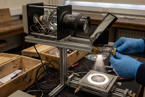
“Semiconductors are like the MMA of engineering,” Bansal says, likening the field to mixed martial arts, where every fighter brings a different discipline. On a deposition tool, Agarwal says to illustrate the point, getting a film to grow with the right crystal orientation is a materials problem, getting the gas to flow evenly is a mechanical one, and controlling both falls to electrical and software engineers. Roughly 100 applications had arrived by launch night, gathered through maker spaces and college clubs. Bansal’s launch post mentions past applicants who have built vacuum chambers to study plasma physics, RISC-V processors (chips based on an open, royalty-free instruction set) from scratch, and scanning tunnelling microscopes. He tells the room about one who built a vacuum chamber because he wants to study nuclear fusion, and who is now fighting his college for the paperwork he needs to buy his materials. “This talent exists in our country, guys,” Bansal exclaims. Lagrange Point has no fab of its own. The organisers say they will take residents to tour labs at IISc, where many would be stepping inside a semiconductor lab for the first time, and will work with IISc labs to test the devices residents make. Any step that needs a full nanofab, Agarwal says, can probably be arranged at IISc or IIT Bombay. HackerFab is an open-source project that began in 2023 at Carnegie Mellon University (CMU) in Pittsburgh, where students design and build cheap versions of the tools used to make chips and publish everything they learn. CMU credits the inspiration to an alumnus, Sam Zeloof, who made chips in his parents’ garage as a high-school student. The company Zeloof later co-founded with the veteran chip designer Jim Keller, now called Fab2, raised $500 million in September at a valuation of $3.7 billion. The IIT Bombay team, founded in August 2025, built a maskless lithography system out of an old projector, a spin coater from a drone motor, a sputtering chamber for laying down metal films, and a furnace that reaches 1,100 degrees Celsius. Swarajya reported in June that the lithography tool cost about Rs 3 lakh in materials, against roughly Rs 1 crore for a research-grade equivalent, and that a full student fab could be put together for Rs 15 lakh to Rs 20 lakh. On 12 June, the team made its first working devices, a diode and a capacitor.
The HackerFab IITB’s team reckons a complete student fab can be built for Rs 15 lakh to Rs 20 lakh
IIT Bombay has made transistors before. Juzer Vasi joined its electrical engineering department in 1981 as its first microelectronics professor, and in the late 1980s a team led by him, with his colleagues A N Chandorkar and Rakesh Lal, built NMOS (n-channel metal-oxide-semiconductor) transistors with features 3 micrometres wide in a cleanroom called Micro-1. They were the first MOS transistors made at any Indian university. Vasi, now a professor emeritus, received the Padma Shri this year, and Bhatia credits his work as the model for what HackerFab is retracing. The patterns the team's lithography tool now prints, 3 to 4 micrometres wide, are close to where Vasi's group worked four decades ago. With the designs public and the costs that low, the founders expected other colleges to copy them within a year or two, but the copying has been slow. Bhatia counts “about 3 or 4” efforts in India. Agarwal says at least two besides IIT Bombay are active. Mahindra University in Hyderabad launched a chapter of its own in August. Agarwal blames belief more than money. “Even if the colleges have funding to start their own HackerFabs, they kind of don’t believe that the kids are capable of making a semiconductor manufacturing tool,” he says. Bhatia describes a second kind of failure, in which a group of students watches the team’s viral YouTube video, builds one or two tools, and stops, “because they don’t know how that fits into the big picture.” A student who has built a working tool in Bengaluru, with industry engineers looking on, would go home with proof that students can do it and a sense of where the work leads. Agarwal sketches a geometric progression in which 20 students start chapters this year and each seeds another. Bansal compares the effort to the early days of the hackathon, a format he and the friends who later founded Lagrange Point pitched to their school principal in Class 9, long before every college ran one. Bhatia does not think India can reach the frontier of chipmaking today. In chip design, he says, a couple of Indian companies are perhaps two years from it, but fabrication cannot be solved in one shot. Rapidus could build a 2 nm pilot line within three years, he says, only because Japan already had an industry around it. Tata Electronics is building a fab at Dholera in Gujarat, with Taiwan’s Powerchip Semiconductor Manufacturing Corporation, for chips from 28 nm to 110 nm, mature generations of the technology. Bhatia would like the government to fund a 2 nm project too. The government has spoken of one. When it announced the second phase of its semiconductor mission in the Budget in February, there was a promise of “a clearly defined roadmap” to 3 nm and 2 nm technology, and that India aimed to be among the top semiconductor nations by 2035. The plan the Cabinet approved in July speaks only of moving to more advanced nodes from a start at 28 nm to 110 nm. But people in the know, Bhatia says, have asked him where such a project would find “the 200 to 500 engineers who have the experience of running a 2 nanometre fab.” They would have to be sent abroad to train and bring the technology back. Even a 2 nm fab, Bhatia argues, would leave India dependent. “If you say that I’m going to go for a 2 nanometre fab, but I’m still going to be dependent on ASML for my lithography machines, I am still going to be dependent on Applied Materials and Lam for the rest of my tools, which are both American companies, then it’s not a complete effort,” he says. ASML, a Dutch company, makes the most advanced lithography machines in the world, and Applied Materials and Lam Research make much of the rest of the equipment in a modern fab. India, Bhatia says, has to go broad as well as deep, starting with what it has. Agarwal puts the frontier at “a 5 to 10 year thing at least”. “You can’t have an Indian equipment company if you don’t have Indian fabs who are willing to buy and qualify their equipment,” he says. A fab spends years qualifying a new tool and will throw up every kind of nakhra (fuss) along the way. Indian design companies, he adds, struggle to get their chips made at the Taiwan Semiconductor Manufacturing Company (TSMC), the foundry that dominates contract manufacturing. “This whole industry is kind of like a mafia,” Bhatia says. “Everyone works with each other and it’s hard for someone to break in.” India, he argues, needs its own version of this mafia, a web of Indian fabs, packaging plants, chemical and materials makers, equipment builders and design houses that buy from and sell to one another. Ashwini Vaishnaw, the Union Minister for Electronics and Information Technology, made a similar case on 14 November. Visiting Ethereal Machines, a Bengaluru maker of advanced machinery and precision components, he said India needed to develop and manufacture its own machines and high-precision components for making semiconductors. The Union Cabinet approved the second phase of the India Semiconductor Mission (ISM) in July, with an outlay of Rs 1,27,500 crore spread across six pillars. One of them is talent, under which industry is to help train people in cleanrooms and fab construction. Another is machines and materials, with incentives for companies that make chip-making equipment, chemicals and gases in India. Agarwal calls the government’s role top-down, setting up fabs and packaging plants with subsidies, and Junction’s bottom-up, making sure engineers exist to run them and companies exist to supply them. Lam Research, Agarwal says, has had to run what amounts to its own version of Junction. Its annual Lam Research Challenge this month drew more than 3,000 students from about 190 colleges through rounds that included building hardware. The government’s Chips to Startup programme, run by the Ministry of Electronics and Information Technology, gives engineering colleges access to commercial chip-design software. It had trained more than 68,000 students across 332 institutions by August, towards a target of 85,000. Students’ designs are pooled onto shared wafers and made into real chips at the Semi-Conductor Laboratory, a government-run fab in Mohali that uses an older 180 nm process. Lam has bet on simulation. In 2024, it began rolling out software that lets students run a virtual fabrication line at 20 Indian universities, with support from the ISM and IISc. Lam and the government expect the programme to train 60,000 people over 10 years. Rangesh Raghavan, who heads Lam Research India, said at the time that there were “only a handful of labs capable of training semiconductor engineers,” and that physical labs could not be scaled. Hands-on training is rarer, and it runs through institutions and companies. In June, President Droupadi Murmu inaugurated a training cleanroom at IISc’s Centre for Nano Science and Engineering, built with the Ministry of Tribal Affairs and expected to train about 700 students a year. Tata Electronics has 300 fresh graduates training at Powerchip’s fab in Taiwan to run its Dholera plant, its chief executive, Randhir Thakur, said in September. Junction asks its residents to build the tools themselves, by hand, which few other programmes in India ask of students. Its nearest relatives are the HackerFab chapters it hopes to multiply. HackerFab’s money has come from SemiX, IIT Bombay’s semiconductor initiative, from the institute’s alumni, and from Emergent Ventures, the grant programme run by the economist Tyler Cowen at George Mason University’s Mercatus Center. Agarwal says the couple of chapters that exist still need to raise money, and the founders are looking at public grants such as those of the Anusandhan National Research Foundation (ANRF). What they want, he says, is student teams still running 20 years from now, and companies that grow out of them. He would count the movement a success if it seeded something like a “PayPal mafia” for Indian semiconductors, the name Silicon Valley gives to the early PayPal employees who went on to found or fund many of its best-known companies. Agarwal has a homegrown precedent in mind. India's electric-vehicle industry, he wrote on X after the launch, drew much of its talent from college racing teams, and Ather Energy, the Bengaluru electric-scooter maker, began, in his telling, with the racing team at IIT Madras. In June, Swarajya reported that HackerFab IITB expected to make its first complete NMOS transistor within weeks. Five months on, the team has not announced one. Its website still lists the transistor as in progress, and at the launch, the founders spoke only of the “first devices” they made in the summer.
In just over a year, HackerFab IITB went from founding to its first working devices.