
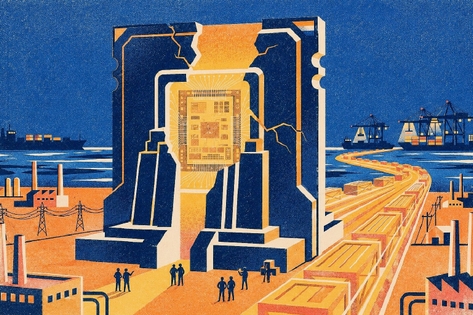
India Has Learnt Chip-Packaging. Can It Build What Goes Inside?
As Amitesh Sinha, CEO of the India Semiconductor Mission and Additional Secretary at the Ministry of Electronics and Information Technology, puts it to Swarajya, “this is a long-term project. At work: Inside CG Semi (PC: Diksha Yadav/Swarajya)Package Inspection: Inside CG Semi (PC: Diksha Yadav/Swarajya)Package Inspection: Inside CG Semi (PC: Diksha Yadav/Swarajya)Air shower protection, a step before entering the lab at CG Semi (PC: Diksha Yadav/Swarajya)CG Semi team (PC: Diksha Yadav/Swarajya)A wafer’s journey through the hall is also a map of the import problem. Saif Alam, programme manager at Kaynes Semicon, says speed at which everything functions is the best part of the Mission. Speed, consistency, transparency, guidance for companies and their foreign partners, and outreach through conferences like the annual Semicon India are, he says, what is working. CG Semi certifies an operator in about four months, one in the classroom and three on the floor, up a four-grade ladder.
Sanand proved an Indian OSAT can be raised at world-beating speed. But beneath the finished package, almost everything is imported — and building that supply chain will take the rest of the decade.
A finished chip package sits on a bench at Kaynes Semicon, in the Gujarat Industrial Development Corporation (GIDC) estate at Sanand. Under its black moulded shell are seventeen dies, six insulated-gate bipolar transistors, six fast-recovery diodes, three more diodes and two controller chips, and seventy-odd bonded wires, some of copper a millionth of a metre and a half thick, some of aluminium, laid down by machines that cost more than the hall they stand in. Almost everything in that shell arrived by ship to Mundra port and from there to Sanand. Some materials reach the plant in trucks built to hold a set temperature, others in trucks with vibration isolation and air-ride suspension. The copper lead frame that carries the dies was rolled in Korea or the Philippines. The bonding wire came from one of two houses, one in Japan and one in Germany, that have supplied the industry for half a century. The epoxy moulding compound that seals it travelled from a plant in Southeast Asia inside a refrigerated truck, because it spoils above minus forty degrees Celsius.
Anatomy of a chip package
Chip Packaging process inside Kaynes Semicon. (PC: Diksha Yadav/Swarajya)
In the last six months, three companies started India’s chip-packaging journey from Sanand. The engineers who run the lines are from across Gujarat, India and the world. Kaynes Semicon shipped India’s first commercially packaged multi-chip modules from its Outsourced Semiconductor Assembly and Test (OSAT) plant to the California firm Alpha and Omega Semiconductor, barely a year after breaking ground. A short walk away, CG Semi, a joint venture that leans on Japan’s Renesas for its manufacturing recipe, cleared formal customer qualification in roughly ten months, against the twenty-odd months the same step takes in Southeast Asia. Micron’s memory-packaging plant opened in February 2026 after a $2.75-billion build. Four years ago none of this stood here, and their second plants are already under construction at Kaynes and CG Semi. An earlier Swarajya report traced how India stood up the three tiers of a chip industry, the design houses, a fab, and the packaging plants known as OSATs or ATMPs, in about four years, and found the tissue connecting them thin to the point of absence. Drop one level below the packaging halls, into the supply chain that has to feed them, and the same problem waits in a more stubborn form. The finished package is a shell of Indian labour wrapped around a core of imported everything. Having the factories was the first step, and ISM 1.0 achieved it. The harder task is building the supply chain that feeds the OSATs and ATMPs, cuts their input costs and makes them price-competitive at home and abroad. As more plants come up, demand for supplies will only rise, and ISM 2.0, which sets out to incentivise the makers and researchers of semiconductor equipment, materials, chemicals and gases, is aimed at exactly this layer. “It will take at least three years to build this supply-chain layer in India, counting the time from ISM 2.0 being notified to project approvals to construction and finally production,” the CG Semi team tells Swarajya. The packaging line is capital, a technology partner and disciplined people, and India can buy or train all three quickly. The harder thing is what has to flow into that line every day, the frames, wire, compound, process chemicals, blades, needles and the qualified vendors who make them, and that ecosystem takes the better part of a decade to build. As Amitesh Sinha, CEO of the India Semiconductor Mission and Additional Secretary at the Ministry of Electronics and Information Technology, puts it to Swarajya, “this is a long-term project. It will take us ten to fifteen years of consistent work, at the same speed, focus and vision, to build a robust semiconductor ecosystem.” India has done the fast, visible, state-controlled half of its semiconductor project with real competence. The slow, market-controlled half is still ahead of it. The government’s ISM 2.0, with a budget outlay of Rs 1.27 lakh crore, is staking its next phase on closing that gap, and on the evidence it is seem to be the right bet. Two roads abroad, and one at home Malaysia opened its first chip-assembly plant in Penang in 1972, when Intel arrived to a fresh free-trade zone. Within a decade a dozen-odd multinationals had followed, and today the country holds close to an eighth of the world’s assembly-and-test business and ranks among the top semiconductor exporters on earth. Fifty years on, it is still overwhelmingly a back-end economy, packaging, testing and the equipment around them, with real wafer fabrication scarce. It is world-class at the back end and has not climbed past it. Taiwan took the other road. Its packaging champion, ASE, was founded in 1984 doing the crudest lead-frame work, listed in 1989 to fund the climb, and reached the top of the global OSAT table by 2003. It did so beside a state that had spent the previous decade absorbing foreign process knowledge, through a technology transfer that began in 1976 and covered packaging and testing as well as wafers, and beside TSMC’s foundry, which guaranteed it volume. India’s own first attempt is the cautionary tale closest to home. In 1984, the same year ASE was founded, the government set up Semiconductor Complex Limited in Punjab, seeded with foreign technology transfers and real ambition. A fire gutted its fabrication plant in 1989 and shut it for the better part of a decade. When it came back, it survived on captive orders from the defence and space programmes and never became commercially competitive. Two ventures began the same year and ended very differently, and the difference was an ecosystem and a market on one side and dependence on government orders on the other. India tried again to attract fabs in 2007 and in 2011, and both efforts collapsed, as industry says, because the ecosystem was not ready. At fourth year of its present attempt, India is now building at every level, from design to fab to packaging to components, and now to the supply chain that feeds the fab and the OSATs. The challenge running through every level is demand, which comes from trusted, established, legacy customers. For a new player to enter at any point in the chain is hard. It is a long process of getting the quality, specifications and processes right, and then convincing the customer that the same quality and quantity will hold, consistently, for years. Every successful back-end industry grew up next to guaranteed volume: ASE next to TSMC, China’s champions next to their domestic foundries, Penang riding Intel’s own output. Sanand’s lines have no such anchor at home yet. India’s fabless startups are too small and too few to feed them, and the Tata-PSMC fab at Dholera is still under construction. So, at the moment Micron packages its own memory chips, Kaynes shipped modules to Alpha and Omega, and CG Semi builds parts qualified through Renesas. Gujarat State Electronics Mission (GSEM) frames the two sites as a single value chain. “While Sanand is a Zero Liquid Discharge (ZLD) estate, in Dholera the government has established a common effluent treatment (CETP) facility which can be used by incoming fabs and supply chain ecosystem companies,” Neha Kumari, mission director of the GSEM, tells Swarajya.
India starts where Malaysia and Taiwan did, but reaches for all three tiers at once.
Two anchors, two routes The two Indian-owned OSAT plants are located at a walking distance from each other in Sanand. Kaynes has taken the independent route. “We are building the country’s only fully integrated electronics manufacturer, one that already assembles boards for Indian OEMs for companies like Maruti Suzuki, TVS, Atomberg, Ola, etc. And now we are integrating backwards into the chip packaging business, and Kaynes Semicon owns the whole thing, we have the complete ownership,” says CEO Raghu Panicker to Swarajya. Kaynes Semicon draws its process from a set of technology partners: AOI Electronics and Fujitsu in Japan, and Globetronics in Penang, the last of which it drew on when it bought power-module production lines from Fujitsu for $13.8 million in June 2025. It sources advanced die-attach materials, silver-sinter films, solder preforms and thermal interface materials, through a partnership with MacDermid Alpha. It runs its imported inputs and gases through the Japanese trading house Mitsui as its supply-chain aggregator. And it has built a research bench that reaches well beyond assembly: statements of work with IBM on flip-chip, interposer and 2.5D and 3D packaging; with Singapore’s A*STAR Institute of Microelectronics on fan-out wafer-level packaging; a photonics-packaging tie-up with XScape Photonics; centres and projects with the IITs at Kanpur, Bombay and Madras, the last working on diamond substrates for power electronics; and Siemens as its package-design training partner. Nobody else in India is treating reliability as a first-order product, Panicker says, and for the automotive customers Kaynes wants, reliability is the whole game. A part that fails in a car is a recall, and the cost is far higher than a return. The company funded the OSAT by going public and stacking the proceeds, some Rs 3,300 crore, on top of the Mission’s capital subsidy, which is the only reason a line this equipment-heavy works out.
The journey of a chip, from a design file to the device in your hand, across six stages and several borders.
Kaynes EMS legacy across India on the Sanand OSAT wall. (PC: Diksha Yadav/Swarajya)
At work: Inside Kaynes Semicon
At work: Inside Kaynes Semicon
Kaynes Semicon team of engineers.
Kaynes Semicon team: on the right are Nanie Torres (GM) and Raghu Panicker (CEO), at the centre is Payal (HR) (PC: Diksha Yadav/Swarajya)
CG Semi has taken the careful route. It is a formal equity joint venture, CG Power of India holding 92.34 per cent, Renesas of Japan 6.82 per cent and Stars Microelectronics of Thailand 0.84 per cent, worth around Rs 7,600 crore. Rather than assemble a process from many partners, it took one partner’s proven recipe wholesale. It sent its engineers and operators to Renesas’s plant in Malaysia for three months to learn the process, then rebuilt it in Sanand under the eye of Renesas counterparts assigned to every step. The CG Semi team describes a qualification cascade worth spelling out. First comes characterisation, establishing the recipe, the order and temperature and pressure of each operation. Then an engineering run to test whether the recipe holds. Then pre-qualification, then formal qualification, each a stiffer repeat of the last, with the technology partner reviewing results at every step before proceeding to the next. Only then does the plant build a customer sample and issue a process-change notification, telling the customer that parts once built at Renesas will now be built in Sanand, which starts a further three-month clock while the customer runs its own tests. The whole sequence takes nine to twelve months. CG Semi says they will use the present plant only to run this process and train its people when their second commercial-scale plant, which is many times larger and now under construction, is ready next year. “Our trial line has already scored above ninety per cent in a Japanese customer’s quality audit and posted yields above the market average, which is the number the company leads with when an American buyer asks why it should come to India at all,” the CG Semi team says. Between them, the two plants describe the choice facing Indian industry: build the capability and own it, assembling it from a spread of partners as Kaynes is doing, or import it whole through a single joint-venture partner and localise it over time, as CG Semi is doing. Both routes run on foreign know-how, and the government has made that easier. The Finance Act of 2025 created a presumptive tax regime for non-resident firms that supply technology and services to set up electronics and semiconductor plants in India.
Each gate is a stiffer repeat of the last, and the whole sequence runs nine to twelve months.
At work: Inside CG Semi (PC: Diksha Yadav/Swarajya)
Package Inspection: Inside CG Semi (PC: Diksha Yadav/Swarajya)
Package Inspection: Inside CG Semi (PC: Diksha Yadav/Swarajya)
Air shower protection, a step before entering the lab at CG Semi (PC: Diksha Yadav/Swarajya)
CG Semi team (PC: Diksha Yadav/Swarajya)
A wafer’s journey through the hall is also a map of the import problem. A wafer arrives, often the customer’s own, and often the single most valuable object on the floor. It is thinned on a backgrinder, mounted, and diced into individual chips, either by a resin blade or, for the thinnest wafers, by a Taiko ring-cut and a stealth laser that scribes beneath the surface. A pick-and-place machine reads the wafer map, lifts only the dies that passed electrical test, and sets each one onto the copper lead frame, the imported frame, fixing it with solder paste, a conductive epoxy or a pressure-sintered silver film for the parts that must shed heat. A wire bonder then stitches the dies to the frame, gold or copper ball-bonds for the fine signal wires and thick aluminium wedge-bonds for the power connections, thousands a minute, each loop shaped to a tolerance finer than a hair. An X-ray and an acoustic scan look for voids. The assembly is cleaned, then encapsulated, for a power module in a vacuum mould that keeps air out of the compound, trimmed of its excess frame, tin-plated, formed into its final leg shape, laser-marked, tested and sorted into bins, and packed into tubes or trays or tape-and-reel for shipping. At almost every station the machine is imported and the consumable is imported: the frame, the wire, the compound, the die-attach film, the dicing blade, the plating chemistry. What India adds, for now, is the labour, the electricity, the water, the building and a few consumables. Packaging is the layer where India has a genuine opening, and the reason is scale. A back-end plant needs perhaps fifteen to twenty gases and chemicals; a wafer fab needs on the order of a hundred and fifty, at the same brutal purity but across ten times the variety. A fab also demands two hundred megawatts of uninterrupted power, twenty million gallons of water a day, and a hundred thousand square feet of cleanroom. An OSAT is lighter on all of it.
At almost every station, the machine is imported and the consumable is imported.
Chip packaging process on the walls of CG Semi (PC: Diksha Yadav/Swarajya)
Why packaging is the opening
The cost is mostly material Cost in this business is mostly material. From what the plants and industry experts describe, material is roughly forty-five to fifty per cent of the total, labour is five or six per cent, equipment, the other great slab of expense, is neutralised by a government subsidy that covers seventy per cent of the capital, and the rest is utilities and maintenance. Cheap power, water at a subsidised rate and cost-effective workforce pull the plant toward competitiveness. Material pushes the other way, because sixty to seventy per cent of it is imported and because the single largest line item, the lead frame, is where India is furthest from making anything at all. Localising it will not, on its own, cut the bill. A May 2026 Niti Aayog study titled 'Future of India's Semiconductor Industry' said that the Indian branches of global suppliers tend to price their products at import parity, tariffs included, so a component “made in India” by a foreign firm’s local arm can cost what the import costs. The competitiveness only arrives when the manufacturing is genuinely Indian and genuinely at scale. This is the arithmetic that decides whether a chip packaged in Sanand can compete with one packaged in Shenzhen, and it is a long-term goal for a country that has only just begun. The material inputs used most in bulk are the copper parts, which constitutes the lead frames, direct-bonded-copper (DBC) substrates and wires, and the moulding compound. If those could be made near the plants in Sanand, it would cut a great deal of cost. Kaynes Semicon and CG Semi both say they are in talks with their suppliers, encouraging them to set up their plant here as the industry is only going to grow. This will not happen immediately, so in the meantime a supplier’s warehouse in Sanand or in the state or in the country would help, cutting transport costs and the unexpected delays that may arise once plants run at full capacity. Imports sort into two tiers, let’s call it the hard and the easy tier. The hard tier is the set of materials that go inside the finished part, the direct materials. ‘The lead frame alone runs to around thirty-five to forty per cent of material cost,’ says Nanie Torres, General Manager at Kaynes Semicon. However, it is not simply copper but a specific alloy grade, stamped to tolerances that take years to master. Then the moulding compound and the die-attach adhesive must be kept below freezing all the way from factory to line, so importing them means paying for a refrigerated cold chain on top of the material. The bonding wire is a market held worldwide by Tanaka Precious Metals of Japan and Heraeus Electronics of Germany. These materials are dominated by a handful of legacy suppliers, to name a few like, Sumitomo and Resonac in compound, Indium and Henkel in adhesive, MacDermid Alpha in the pressure-sintered silver the newest power modules need, who sell qualified, trusted products a customer will not let an OSAT swap out on a whim. Even if a supplier agrees to set up a plant, it is a three-year project at best. The realistic near-term step is smaller: persuade those suppliers to hold stock in an Indian warehouse rather than ship each order across an ocean, and Kaynes and CG Semi say some of the players are already planning exactly that. ISM 2.0 may speed things up for them.
Assembly process on a screen at Kaynes Semicon (PC: Diksha Yadav/Swarajya)
Material cost pushes against competitiveness; cheap power, water and labour pull the other way.
The easy tier, and who can enter it The easy tier is everything else, “it is where the opening for Indian small and medium firms lives. Facility chemicals, the sodium hypochlorite and cooling-tower and water-treatment chemistry used to keep the plant running rather than built into the part, India already makes,” says Pranav Vijayakumaran Nair, business finance and analysis head at Kaynes Semicon. The trays and tubes and tape-and-reel the finished chips ship in, the nitrogen storage cabinets and lead-frame racks, the metal fabrication around the line, the packaging boxes and pizza-shaped trays, some of these Kaynes and CG Semi are already localising with Indian fabricators. And the entire apparatus of the clean room, the gloves, masks, gowns, lint-free paper and anti-static mats, is made in India already. “The country’s mature pharmaceutical industry, especially injectables, has been building and supplying clean rooms for years. A semiconductor clean room is, from the outside, an unusually advanced pharma clean room, and India knows how to dress one,” says CG Semi team. Gases are handled well, though not effortlessly. INOX Air Products, a joint venture between INOX and the American firm Air Products and Chemicals, had made oxygen, nitrogen, argon, hydrogen and helium for decades, but semiconductor-grade meant far tighter purity and, as its head of business development Diganta Sarma tells Swarajya, consistency day after day matters as much as purity itself. The firm invested in advanced purification, parts-per-billion/parts-per-trillion (PPB/PPT)‑level analytics and dedicated filling to get there, and where a grade is not yet made in India it draws on its American parent. “We are building onsite plants and facilities right in Sanand to support one of the first global semiconductor companies setting up there, while continuing to supply from our established base in Ahmedabad. At the same time, our Electronic Specialty Gas Hub in Dholera will serve as a national nerve centre for semiconductor gases and logistics. India’s semiconductor journey will be measured in decades, not years, and we are investing ahead of demand with India’s first 6N ultra‑high‑purity liquid oxygen facility, the first electronic‑grade nitrous oxide plant, and a new Dholera hub for electronic gases,” Sarma adds. “Homegrown chemical makers are moving too. HySpec Chemicals, a technology-led specialty chemicals company promoted by Deepak who is the Chairman and Managing Director of Deepak Nitrite, signed an MoU with the Gujarat government on March 1, 2026, at the Gujarat SemiConnect Conference. They have committed around Rs 750 crore to semiconductor-grade gases and chemicals,” Ms Kumari tells Swarajya. Gujarat has traditionally been strong with the chemicals ecosystem, and the state’s electronics policy already offers capital and operating support for production of semiconductor-grade gases and chemicals. The CSIS report on India’s ecosystem, published in April 2026, notes that firms now find indigenous supplier options better in quality and more diverse than at the Mission’s first phase in 2023. The easy tier is filling. Between the tiers sits a long tail of consumables, the diamond blades that dice the wafer, the needles that push each die up from below, the rubber tips that lift it into place, the “pizza box” trays and green lint-free paper of the clean room, the anti-static footwear and mops. These are the places where a small firm can meet the specification, clear the anti-static and particle requirements, and enter. And it is already happening. A retired army officer who wanted to build a factory for shipping reels for packaged chips two kilometres away from the plant in Sanand have been inquiring of the possibilities. He has taught himself about the product at semiconductor trade shows, found a Taiwanese firm to supply the technology, and could hold forth on reel thickness when he approached Indian firms. Like INXOAP and Linde India, country already has a plating-chemical maker in Atotech India, in Gurugram, and a silver-epoxy and solder-paste capability in MacDermid, in Chennai as well. But when it comes to smaller firms, “the appetite is real, if still early,” Vinod Kumar, honorary president of the India SME Forum tells Swarajya adding, “serious enquiries have risen sharply over two years, from firms already in precision engineering, speciality chemicals, industrial gases, cleanroom equipment, tooling and automation, and that ISM 2.0 shifted the question from whether India can build fabs to how Indian firms can supply them. Most are eyeing the lower-barrier tier, the machining, consumables, packaging, tooling, testing and logistics where they already have expertise. Far fewer are looking at electronic-grade chemicals, ultra-high-purity gases, wafers, photoresists or bonding wires, where the technology barriers and qualification cycles are steep.” Only a small share are investment-ready today; many are still assessing where their strengths fit. Interest is strongest, Kumar shares, among firms already supplying aerospace, defence, automotive electronics and medical devices, whose quality systems are closest to what semiconductors demand. India’s incentive architecture began as capital subsidy, the Mission covering half the cost of a fab or an OSAT and a scheme called SPECS a quarter of the cost of a component plant. That suits the big, capital-heavy players. The newer Electronics Component Manufacturing Scheme, approved in March 2025, is built differently. It is performance-linked, rewarding revenue and jobs rather than capital spent, and aimed at the components and sub-assemblies where entry barriers are low. A separate production-linked scheme for passive components, launched the same month, takes aim at a projected $248-billion supply gap. These are the instruments that could move a reel-maker or a blade-maker this year rather than in the 2030s, if the money reaches the small firms it is meant for. A small firm cannot afford the legal muscle to interpret rules that change every quarter, and being brought inside the Mission’s single-window clearance is, for such a firm, as valuable as any subsidy.
INOX Air Products' Dholera project in the making.
The easy tier is where the opening for Indian small and medium firms lives.
Qualification, the real wall The reason the hard tier is hard, and the reason even the optimists put a ten-to-fifteen-year horizon on a mature ecosystem, comes down to one word that recurs on the Sanand floor: qualification. A new material cannot merely be cheaper and good enough. It has to be approved, by the OSAT, then by the OSAT’s customer, then often by the customer’s customer, through a testing cycle that runs one to two years and runs longer and stiffer for anything destined for a car, where the incumbent is almost never displaced. A facility takes at least a year and a half to build, a few more months to set up and hand to the customer, and about a year for the customer to align and approve, which is why any serious localisation lands around the three-year mark, whether the supplier goes it alone or through a joint venture, says CG Semi team. The India SME Forum sees the same wall. Capital matters, Kumar says, but qualification has emerged as the larger challenge. A SME firm can upgrade its plant and still spend twelve to twenty-four months on customer audits, validation and reliability testing before a first commercial order, funding itself through that pre-revenue stretch. Many smaller firms now rate qualification support, customer access and technical mentoring as highly as capital subsidies, and want working capital, shared testing facilities and visible future demand before they commit. The most deflating proof of how sticky this is comes from Torres, who spent thirty-five years in the industry across the Philippines and Malaysia before coming to Sanand. The bonding wire, he points out, still comes from Tanaka and Heraeus even in Malaysia and the Philippines, decades into their back-end industries. Mature, world-class hubs, still buying the same wire from the same two firms after half a century. A CG Semi strategist puts the same point: semiconductor technology can be learned, he says, but a supply chain is very hard to replicate, because supply chains are sticky, and whether India’s ecosystem succeeds will depend on how much of that hidden, hard-won web it can attract and hold. The relationships beneath the factories have to be grown. The state’s half If the ecosystem is the slow half, the state’s execution has been the fast half. Mr Sinha explains that under the Mission (ISM), government money is concurrent with private investment. The model is pari passu: the applicant spends, the state government matches, the Mission matches, all three tranches moving together. “This pari passu funding model is the most crucial factor in why this scheme has worked well,” says Kaynes’ Panicker adding that, once all approvals are done, funding comes within few days, not even a week. PM Narendra Modi has been to Sanand for each of the three inaugurations. While attending the CG Semi’s inauguration that enter commercial production on 4 July 2026, PM Modi quoted a Gujarati saying which he believes in and resonated well with the crowd, and it stuck with me: “નિશાન ચૂક માફ, નહીં માફ નીચું નિશાન. Lakshya humesha bade rakho, main Lakshya humesha bade rakhta hun, nishan chuk hoga toh dekhenge”. In English the saying translates to “Missing the target is forgivable, aiming low is not.” This also reflects in how Gujarat functions. The state already has a total of six semiconductor projects now, of which some are under construction: Micron Technology, Kaynes Semicon, CG Semi, Tata Electronics + PSMC fab, Suchi Semicon, and Crystal Matrix Limited. Saif Alam, programme manager at Kaynes Semicon, says speed at which everything functions is the best part of the Mission. There are no bureaucratic hurdles or delays, from the ground level to the top, everyone is quick to address a query. “For example, the GST refund process happens within twenty-eight days, but once we had a shipment urgency and the state government was prompt to address our request, we got the refund in two days. The government’s approach to the semiconductor sector has truly redefined ease of doing business.” Asked what sets the Mission apart, Mr Sinha says: a number of things, the pari passu funding, the coordination at every level from the state to the Prime Minister, and a policy implemented on the ground line by line as it appears on the Mission portal, with no back-door meetings and no company-to-company variation. Speed, consistency, transparency, guidance for companies and their foreign partners, and outreach through conferences like the annual Semicon India are, he says, what is working. CG Semi and kaynes Semicon points to concrete regulatory wins that few others mention. In the special-economic-zone accounting, the commerce ministry agreed that the imported wafer, around ninety per cent of a chip’s value and always owned by the customer, should be excluded, so the OSAT is measured only on the ten per cent of value it adds. The land threshold for a semiconductor SEZ was cut from fifty hectares to ten. When customs wanted to open sealed equipment that can only be unboxed inside a clean room, the government agreed to let it be opened in the clean room instead. The rules were written before semiconductors existed in India, and officials are now updating them at every level.
PM Narendra Modi at CG Semi inauguration (PC: Diksha Yadav/Swarajya)
ISM CEO Mr Amistesh Sinha (From X)
However, some work remains, and soon will resolve as firms and officials are working towards it. Gold bonding wire is still treated as a precious-metal import needing special handling and security checks, rather than as a raw material for the industry, the way every competing country treats it. Spare parts and repairs for tools from Europe or Japan take time, so a service centre in India, or in Gujarat, would save both. The hope is that ISM 2.0 pulls material and equipment suppliers to at least set up warehouses and service centres in India, and in the Sanand cluster, which would save the chip packaging firms time and money. There is a clearance issue too sometimes, like when a tool goes out for repair and a spare part comes in exchange for temporary use, no purchase happens and there is no invoice, but because officials read the spare as a new product, clearing it becomes a task. Right now, the ISM and the GSEM actively coordinates with the relevant departments to remove such barriers in time, but the government is also working on standard solutions to make the process more seamless. The April 2026 CSIS report titled 'Expanding India's Role in the International Semiconductor Ecosystem" describes the same friction from outside: equipment is sometimes classified differently depending on the port it enters, sometimes because customs officers lack the product knowledge, and some tools are more advanced than anything imported before, which brings delays and overcharges. Better training and clearer corresponding Harmonised System Codes, it suggests, may help prevent the need for escalation and customs appeals for reclassification. The state’s speed shows in Gujarat’s own machinery. Gujarat was the first state to bring out a dedicated semiconductor policy after the Centre’s, and it created GSEM specifically to fast-track approvals and run a single window for the industry, says Ms Kumari. “The mission coordinates with more than fifty departments and holds weekly reviews so that a company does not run from one office to the next. When Micron arrived, GSEM helped bring some of its suppliers on board and tied up the pollution-control and other clearances.” The point, she says, is that an investor should see one government, not a maze of verticals. ISM 2.0 works on a six-pillar approach in which suppliers, of gases, chemicals, equipment and ecosystem services, are a major part, and Gujarat plans to supplement its own policy in step. The state has already drawn interest from gas and material suppliers, INOX, Linde, TNSI, Air Liquide and Fujifilm chief among them, with land allotted to some, and a vendor park with a free-trade warehousing zone is in the final approval stages at the Dholera investment region to house suppliers and ecosystem partners. “As the industry is expanding, we (GSEM) have also expanded our team now so the coordination remains smooth and every case is treated as priority, big or small,” Ms Kumari adds. A cluster becoming a city The pace shows, too, in how Sanand is being built as a place to live and work. Ms Kumari explains the choice of Sanand. It was already a two-thousand-hectare GIDC estate with plug-and-play power, water and roads and existing industries in automobiles and pharmaceuticals, thirty-five kilometres from Ahmedabad, from which workers could travel. The estate’s industrial story began with the Tata Nano: after farmer protests forced the small-car plant out of Singur in West Bengal in 2008, Gujarat gave Tata land at Sanand within days, and the first Nano rolled out in 2010, turning farmland into an auto hub. The chip plants stand on that ground. Under the Gujarat Semiconductor Policy of 2022, with single-window facilitation through GIDC and arrangements for semiconductor-grade water and dedicated power, the state is turning the town into a cluster city. GSEM has allotted land near Sanand to OSATs & ATMP for dormitories, with construction due to begin, because the anchors intend a majority-female workforce. Right now, the workers travel from Bopal and Shilaj, the place has good housing, restaurants, shopping complexes and other amenities that Sanand still lacks, which is almost an hour away from the plants. The state-run ESIC is building a dedicated hospital in Sanand, and hotels are coming up, a Marriott among them. An electronics-manufacturing cluster is taking shape around the packaging plants. Micron’s plant already has two or three vendors nearby, Nippon Sanso for specialised gases among them, the way Penang’s suppliers once clustered around Intel, the first faint sign that the anchor-pulls-the-supply-chain model can work here too. The state government has initiated reforms in the legislation to enable women to be employed across 24-hour shifts, with necessary safeguards. As reported in December 2025, with nearly 70 per cent of the semiconductor facility staff being women, local authorities are dedicating ₹15 crore to advanced surveillance (such as high-end drones) and modernized security across Sanand and Dholera. GIDC Sanand spans more than 2,000 hectares with over 900 industries. “An area more than 500 acres is earmarked to be developed as Electronics Manufacturing Cluster meant to pull in packaging, component makers, materials, precision engineering and EV electronics to co-locate with the anchors,” says Ms Kumari of GSEM. The talent pipeline that seemed impossible two years ago is materialising, through the industrial training institutes whose graduates make up most of the operator workforce, and through company courses in engineering colleges. CG Semi certifies an operator in about four months, one in the classroom and three on the floor, up a four-grade ladder. Two of Kaynes’ 2025-batch female engineers from Gandhinagar, Tanya and Deepa, say they chose VLSI design as one of the subjects in their second-year after learning at a Vibrant Gujarat event in 2023 about the sector. They later took the month long Kaynes Semicon’s online course in their fourth year. College juniors now call us often to ask how to get in, what subjects to take, and seeing the Prime Minister visit Sanand several times has made them keener still to join the sector, the engineers tell Swarajya. GSEM also runs SemiConnect, an annual event with round tables for Japan, Taiwan and the anchor firms. The Gujarat government has taken up several initiatives for workforce development including - the first of its kind Semiconductor assembly and packaging training centre at PDEU in Gandhinagar, that delivers industry-led and industry-focused skills on actual production grade equipment run on actual process and consumables. It is also supporting the development of a nano fabrication lab SAMARTH at IIT Gandhinagar which will be Silicon and Advanced Manufacturing Research and Training Hub, says Ms Kumari. More on how the talent and the workforce is being built in the country will be coming up in the next article. Foreign trainers, Korean, Filipino and Malaysian veterans on three-to-five-year stints, are teaching a workforce that will soon be almost entirely Indian.
Vibrant Gujarat Regional Conference 2026: MoU signed between FUJIFILM India and the GSEM. (In picture: Neha Kumari, GSEM Director)
Gujarat SemiConnect Conference 2026: One of the meeting focused on strengthening the semiconductor ecosystem in the state and enhancing industrial partnerships with Japan.


© All Rights Reserved.