The Dholera fab is being built for the seventy.
Why, the argument runs, would a country with twenty per cent of the world's chip designers settle for legacy silicon?
A "transistor" on a 3nm chip is a complex three-dimensional structure whose smallest features still measure well over ten nanometres — the headline number is a generational marker, not a ruler reading.
A 28nm fab costs ten to fifteen billion dollars to set up; a 3nm fab roughly twenty billion; a 2nm fab is projected at twenty-eight.
TSMC took 35 years to climb from 3 micron to 3nm; SMIC took 22 years to reach 7nm-class production.
Seventy per cent of the global wafer market lives at 28nm and above; the three per cent that lives at 3nm is where the headlines spend their attention. The Dholera fab is being built for the seventy.
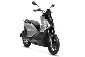
On 16 May 2026, Narendra Modi stood inside the headquarters of ASML in the Dutch town of Veldhoven and witnessed the signing of a strategic partnership between the lithography company and Tata Electronics. ASML is the only firm in the world that makes extreme-ultraviolet lithography machines, the most expensive piece of industrial equipment ever serially produced, without which no chip below about 7-nanometre process technology can be manufactured at scale. The agreement committed ASML to supplying lithography systems, technical training and ecosystem support to Tata's new semiconductor fab at Dholera, Gujarat — India's first commercial fab, a ninety-one-thousand-crore-rupee facility being built with Taiwan's Powerchip Semiconductor Manufacturing Corporation, expected to produce its first sellable wafers in late 2026. The fab will not use EUV. The chips it produces will be, in the main, 28-nanometre chips, with capacity also for the older 40, 55, 90 and 110-nanometre nodes — the workhorses of automotive electronics, power management, displays, sensors, telecom radios and the embedded silicon of industrial life. The number on the marketing material reads twenty-eight, and twenty-eight is the number this country needs. This has been read in some quarters as a disappointment dressed up as an announcement. Coverage on social media and in parts of the trade press has greeted Dholera's node choice with a particular sneer reserved for technology hesitation: that India, having finally got the capital, the political will, the foreign partner and a signed deal with the Dutch lithography monopoly, has chosen to start at a node the bleeding edge of the industry crossed back in 2011. Why, the argument runs, would a country with twenty per cent of the world's chip designers settle for legacy silicon? Why not chase 3nm, or at least 7nm, the way China's SMIC has? Why announce a fab whose process technology is older than some of the engineers who will operate it? The question contains its own answer if you look at it from the right angle. The 28-nanometre choice is the only entry point that combines a real market, an achievable execution path, a defensible geopolitical position and a finite capital bill — and the historical record of every successful semiconductor nation says you do not skip it. India, after almost half a century of failed attempts to build a commercial fab on its own soil, has finally chosen the starting line that someone serious would actually pick. The error in the criticism is the assumption that there is a shortcut. There isn't. The seventy per cent of the global wafer market that lives at 28nm and above is where India's industrial economy actually spends its import dollars; the three per cent that lives at 3nm and below is where the headlines spend theirs. To mistake one for the other is to confuse the silicon with the celebrity.
Roughly 70 per cent of global wafer volume sits at 28nm and above — the mature nodes that power automotive, telecom, defence and the embedded silicon of industrial life. Only 3 per cent sits at 3nm and below. Dholera is being built for the seventy.
To see why this matters, you need to understand what the number on the marketing material refers to. The "nanometre" in 28nm originally meant something physical — the width of the smallest features the fabrication process could etch onto silicon. Smaller features mean smaller transistors, which means more computing power per square millimetre and less power burned per operation. Around the 22nm generation, the numbers stopped being literal measurements and became marketing labels. A "transistor" on a 3nm chip is a complex three-dimensional structure whose smallest features still measure well over ten nanometres — the headline number is a generational marker, not a ruler reading. What they still index accurately is cost. A 28nm fab costs ten to fifteen billion dollars to set up; a 3nm fab roughly twenty billion; a 2nm fab is projected at twenty-eight. ASML's High-NA EUV scanner, the machine that prints the most advanced circuits, costs three hundred and eighty million dollars per unit, weighs as much as two Boeing 777s and takes six months to install. It is sold under Dutch export controls tightened in September 2024 to cover even older immersion DUV systems bound for China. This is the territory the critics want India to enter. Set aside whether the country can afford it; even if it could, the bigger question is whether anyone would buy the chips. The chip in a Bajaj Chetak's battery management system sits at a mature node. So does the microcontroller in a Tata Nexon EV, the power IC in a domestic UPS, the signal processor in BEL's through-wall radar and the analog front-end in a Tejas Networks 4G radio mounted on a BSNL tower. Renesas, the Japanese automotive chip giant, launched a flagship vehicle-control microcontroller in March 2026 — the RH850/U2C — at 28nm. The chips India's economy actually buys, in their billions, sit at twenty-eight nanometres and above. TrendForce's foundry forecasts put mature-node capacity at roughly seventy per cent of global wafer volume; the US Bureau of Industry and Security found in December 2024 that about eighty per cent of the semiconductors inside a modern car sit between 28 and 180nm. A single passenger vehicle now contains between fourteen hundred and three thousand chips. The shortage that brought the global auto industry to its knees in 2021 was a shortage of mundane microcontrollers and power-management ICs at mature nodes. Maruti Suzuki cut production by 51 per cent in September 2021 alone. The Indian auto industry lost something in the region of twenty-five thousand crore rupees in sales that year because of chips it could not get. Those chips were 28nm and 40nm and 65nm and 90nm. None of them were 3nm.
Between 1,400 and 3,000 chips sit inside a single modern passenger vehicle, with eighty per cent at 28–180nm. Maruti Suzuki cut production by 51 per cent in September 2021 alone; the Indian auto industry lost roughly ₹25,000 crore in sales that year. None of the missing chips were 3nm.
The deeper case for Dholera is historical. Every nation that built a successful semiconductor industry began at the trailing edge of its era and climbed the node ladder, slowly, over decades — and the nations that tried to skip the climb failed. TSMC was founded in February 1987 at the 3-micron node, three thousand nanometres, roughly a hundred times slacker than what Dholera will start with. It took TSMC twenty-four years to reach 28nm in 2011, thirty-five to reach 3nm in 2022, on cumulative capex now exceeding three hundred billion dollars. Samsung entered semiconductors in 1974 and reached 14nm logic only in 2015. SMIC, China's national champion, was founded in 2000 at 180nm and produced its first 7nm-class chip — the Huawei Kirin 9000s, made through DUV multi-patterning — in August 2023, twenty-two years later, backed by forty-five billion dollars of Big Fund subsidies and the world's largest captive demand pool.
TSMC took 35 years to climb from 3 micron to 3nm; SMIC took 22 years to reach 7nm-class production. Both began at the trailing edge of their era. Dholera is now taking its first step onto the same ladder.